Giỏ hàng
0 Sản Phẩm

2.048.475₫
Designed and Tested to meet JEDEC
Free Technical Support
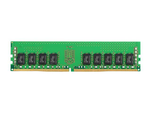
| Brand | Kingston |
|---|---|
| Series | Value |
| Model | KVR24R17S4/8 |
| Capacity | 8GB |
|---|---|
| Type Type | 288-Pin DDR4 SDRAM |
| Speed Speed | DDR4 2400 (PC4 19200) |
| CAS Latency CAS Latency | 17 |
| Timing Timing | 17-17-17 |
| Voltage Voltage | 1.20V |
| ECC ECC | Yes |
| Buffered/Registered Buffered/Registered | Registered |
| Rank | 2Rx4 |
| Chipset | Major Brand Chipset |
| Heat Spreader | No |
| Features | Power Supply: VDD = 1.2V (1.14V to 1.26V)
VDDQ = 1.2V (1.14V to 1.26V) VPP – 2.5V (2.375V to 2.75V) VDDSPD = 2.25V to 2.75V Functionality and operations comply with the DDR4 SDRAM datasheet 16 internal banks Bank Grouping is applied, and CAS to CAS latency (tCCD_L, tCCD_S) for the banks in the same or different bank group accesses are available Data transfer rates: PC4-2400, PC4-2133, PC4-1866, PC4-1600 Bi-Directional Differential Data Strobe 8 bit pre-fetch Burst Length (BL) switch on-the-fly BL8 or BC4 (Burst Chop) Supports ECC error correction and detection On-Die Termination (ODT) Temperature sensor with integrated SPD This product is in compliance with the RoHS directive. Per DRAM Addressability is supported Internal Vref DQ level generation is available Write CRC is supported at all speed grades CA parity (Command/Address Parity) mode is supported |
|---|
| Date First Available | November 13, 2020 |
|---|


NGUỒN HÀNG ĐẢM BẢO
Hàng hóa trên HQG.VN được bán bởi các các nhà cung cấp lớn và uy tín nhất thế giới.

GIÁ CẢ CẠNH TRANH
HQG.VN đem đến cơ hội mua sắm hàng hóa chất lượng quốc tế, giá Việt Nam cho tất cả mọi người.

GIAO HÀNG TOÀN QUỐC
HQG.VN giao hàng miễn phí tới tất cả 63 tỉnh thành trên toàn quốc.

THANH TOÁN THUẬN TIỆN
Hỗ trợ nhiều phương thức thanh toán. Được đảm bảo an toàn tuyệt đối bởi nganluong.vn

BẢO HÀNH SẢN PHẨM
HQG.VN có chính sách bảo hành chính hãng cho các sản phẩm

HỖ TRỢ 24/7
Tổng đài hỗ trợ: 028.7309.6999
Bảo hành 24/7: 1900636106
| Brand | Kingston |
|---|---|
| Series | Value |
| Model | KVR24R17S4/8 |
| Capacity | 8GB |
|---|---|
| Type Type | 288-Pin DDR4 SDRAM |
| Speed Speed | DDR4 2400 (PC4 19200) |
| CAS Latency CAS Latency | 17 |
| Timing Timing | 17-17-17 |
| Voltage Voltage | 1.20V |
| ECC ECC | Yes |
| Buffered/Registered Buffered/Registered | Registered |
| Rank | 2Rx4 |
| Chipset | Major Brand Chipset |
| Heat Spreader | No |
| Features | Power Supply: VDD = 1.2V (1.14V to 1.26V)
VDDQ = 1.2V (1.14V to 1.26V) VPP – 2.5V (2.375V to 2.75V) VDDSPD = 2.25V to 2.75V Functionality and operations comply with the DDR4 SDRAM datasheet 16 internal banks Bank Grouping is applied, and CAS to CAS latency (tCCD_L, tCCD_S) for the banks in the same or different bank group accesses are available Data transfer rates: PC4-2400, PC4-2133, PC4-1866, PC4-1600 Bi-Directional Differential Data Strobe 8 bit pre-fetch Burst Length (BL) switch on-the-fly BL8 or BC4 (Burst Chop) Supports ECC error correction and detection On-Die Termination (ODT) Temperature sensor with integrated SPD This product is in compliance with the RoHS directive. Per DRAM Addressability is supported Internal Vref DQ level generation is available Write CRC is supported at all speed grades CA parity (Command/Address Parity) mode is supported |
|---|
| Date First Available | November 13, 2020 |
|---|